Ion implantation advances Ga2O3 power transistors
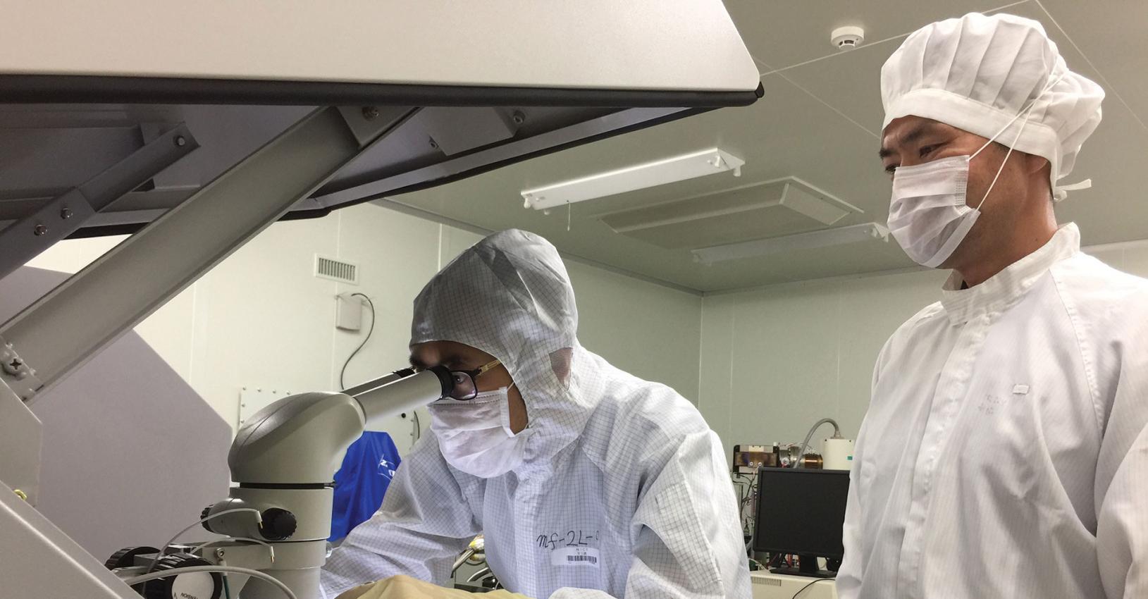
By providing p-type doping, nitrogen-ion implantation promises to accelerate the development and commercialisation of vertical gallium oxide transistors
BY MASATAKA HIGASHIWAKI AND MAN HOI WONG FROM THE NATIONAL INSTITUTE OF INFORMATION AND COMMUNICATIONS TECHNOLOGY
To combat climate change, we need to generate far more clean electricity, and use this precious resource far better. Improvements must be made in motor drives, electrified transportation, data centres and the grid.
In all these applications, the performance of the power converters is governed by the characteristics of two core components: the diode, which controls the direction of current flow; and the transistor, which acts as a switch. Today, the majority of diodes and switches are made from silicon, but they are rapidly approaching fundamental performance limitations. Due to these constraints, commercial power systems are bulky and inefficient. What’s needed is the emergence of a portfolio of wide-bandgap semiconductors that will define a new generation of design for power conversion.
One material that has recently earned its citizenship within the compound semiconductor community is gallium oxide. Its hallmarks include an incredibly large bandgap that makes it a very promising candidate for high-voltage, high-power device applications, and the availability of large-size, high-quality wafers produced from melt-grown bulk single crystals. In addition to these two very attractive features, it is easy to dope Ga2O3 by ion implantation. This is a rare, yet technologically desirable property for any compound semiconductor.
For mass production of silicon and SiC devices, a key technology is ion-implantation doping. Its merits, compared with alternative process technologies such as re-growth and diffusion, include a higher degree of freedom and a considerable cost advantage for designing device structures.
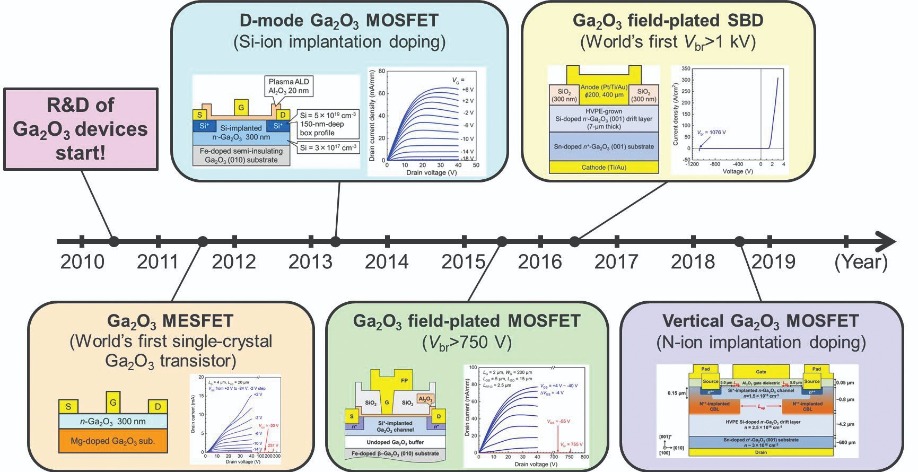
Figure 1. R&D history of Ga2O3 transistors and Schottky barrier diodes at NICT.
Working at the National Institute of Information and Communications Technology (NICT), Japan, our team has been pioneering the development of Ga2O3 devices. Highlights include the ground-breaking demonstration of the world’s first single-crystal Ga2O3 transistor. This success has galvanized intensive international research activities into the science and engineering of this class of material.Weaknesses of the first Ga2O3 transistor, a metal-semiconductor field-effect transistor (MESFET), include large ohmic contact resistances for the source and drain electrodes. In addition, this device is held back by a lack of uniform, reproducible, n-type tin doping of the MESFET channel during crystal growth. This impediment stems from a narrow growth temperature window, making it very difficult to promote dopant incorporation into the material while maintaining high crystal quality.
To improve our MESFET, we have developed a silicon-ion implantation doping process. This allows us to trim the ohmic contact resistance by selectively forming heavily n-type Ga2O3 regions that shorten the metal–semiconductor tunnelling barrier thickness. Further benefits are that by using silicon-ion implantation for doping of the channel layer, we can employ higher growth temperatures that ensure optimal crystal quality – no longer do we have to worry about the possibility of irreproducible dopant profiles.
Thanks to development of our ion-implantation technology, we have been able to realise several milestones in Ga2O3 device technology. They include: depletion-mode MOSFETs; the world’s first Schottky barrier diodes with a breakdown voltage of over 1 kV; enhancement-mode MOSFETs; and very recently, vertical depletion-mode (D-mode) MOSFETs (see Figure 1).
Ion implantation doping
Most of our effort at developing n-type ion implantation doping of Ga2O3 has involved the addition of silicon. It forms a shallow donor, and with an activation energy below 50 meV, full dopant ionization is realised at room temperature. Typically, we activate the implanted silicon atoms with annealing at 800 - 1000°C. Even at these relatively low temperatures compared to those used to activate dopants in SiC, activation efficiency is really high: it is almost 100 percent for a silicon doping concentration of 1017 - 1018 cm-3, and between 60 percent and 80 percent for a concentration of more than 1019 cm-3.
While n-type doping is relatively easy, p-type doping is anything but. This has led the Ga2O3 community to endure a long struggle to uncover a suitable p-type dopant. Now, at last, the wait is over – recently, we have succeeded in developing an effective p-type ion implantation doping process using nitrogen as an acceptor.
Note, however, that it is not possible to obtain p-type Ga2O3 with effective hole conductivity. There are fundamental reasons why this is the case. One reason is that Ga2O3 lacks shallow acceptors with activation energies that are sufficiently small for ionisation at room temperature. According to several independent theoretical calculations, typical acceptor candidates for Ga2O3 – such as magnesium, zinc, beryllium and nitrogen – all have activation energies of 1 eV or more.
Additional reasons behind the lack of p-type Ga2O3 are related to its valence band structure, which is composed of oxygen 2p orbitals. Due to a very small dispersion in the band structure, holes have a very large effective mass – and calculations indicate that these positive charge carriers are impeded by a self-trapping effect associated with characteristic lattice distortions.
However, there is still a limited role that p-Ga2O3 can play – it is useful for engineering large energy barriers in the form of p-n junctions. We have done just that, with experiments confirming that a nitrogen-ion implanted Ga2O3 region formed in n-Ga2O3 can act as a current-blocking layer.
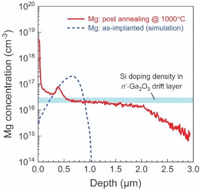
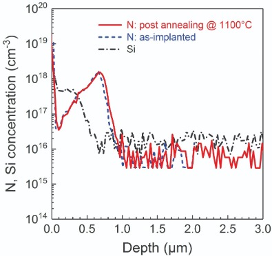
Figure 2 . Depth profiles of implanted (a) magnesium and (b) nitrogen atom concentrations before and after thermal activation annealing at 1000°C and 1100°C, respectively. All profiles were measured by secondary-ion mass spectrometry (SIMS), except for the simulated as-implanted magnesium profile. After annealing at 1000°C, the as-implanted Gaussian-like magnesium profile was transformed into a box-like one with a plateau concentration stabilised at the background donor concentration. On the other hand, absence of thermal diffusion was confirmed for implanted nitrogen atoms even after 1100°C annealing.
During the last few years, we have devoted much effort to developing a p-type ion implantation doping process for Ga2O3. We began by investigating magnesium, the dopant used in GaN. We were encouraged by the high degree of activation after annealing at a relatively low temperature of 900 - 1000°C. However, significant thermal diffusion of these implanted atoms took place immediately.The background donor density determined the final distribution of the magnesium ions. Due to this, the as-implanted Gaussian-like magnesium profile transformed into a box-like profile, with a plateau concentration that was stabilised at the background donor concentration (see Figure 2(a)). We found that this happened for various concentrations of magnesium and the background donors, such as silicon and tin. Therefore, its occurrence was independent of both the impurity concentrations and the specific donor species.
Due to the rapid diffusion of magnesium, we switched to nitrogen, which is theoretically predicted to be an acceptor in Ga2O3, for p-type ion-implantation doping. The good news is that implanted nitrogen atoms are activated above 1100°C, and that thermal diffusion is insignificant compared with magnesium (see Figure 2(b)).
We have compared the current-blocking characteristics of magnesium- and nitrogen-doped Ga2O3 barrier layers fabricated in n-Ga2O3 by ion implantation and subsequent activation annealing (see Figure 3). Our measurements reveal that the current-blocking capability of the nitrogen-implanted barrier layer is vastly superior to that of the magnesium-implanted equivalent. For the nitrogen-implanted structure, the distribution of nitrogen atoms after the annealing process is nearly identical to the as-implanted profile; as a result, an n-p-n junction structure can be formed in the n-Ga2O3, and the nitrogen-doped p-Ga2O3 region can block electron current flow due to a large built-in potential at the n-p junction.
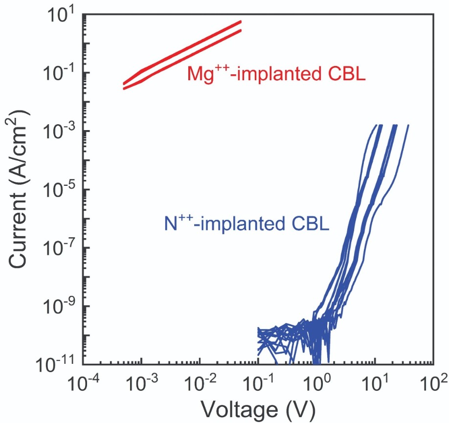
Figure 3. Comparison of vertical leakage current through nitrogen-implanted and magnesium-implanted current-blocking layers. The nitrogen-implanted region led to a much lower leakage current than the magnesium-implanted one.
With a magnesium dopant, it’s a different state of affairs. Due to thermal diffusion during the annealing process, the profile of the magnesium atoms is stabilised at approximately the background donor concentration. The concern is that this could compromise the carrier compensation effect of magnesium implantation, leading to the formation of an n--region instead of a p-region, and culminate in the creation of an n-n- junction of minimal barrier height. The conclusion is clear: nitrogen is more useful than magnesium as an acceptor for the ion implantation process to make p-type Ga2O3, at least for the purpose of forming an energy barrier in n-Ga2O3.Vertical transistors
We have employed our nitrogen-ion implantation doping process when fabricating normally-on D-mode vertical Ga2O3 MOSFETs. These transistors have a vertical architecture, because this is superior to a lateral one for realising high voltage ratings and high power levels. What’s more, it allows higher currents without requiring sizeable layout areas, and it enables far superior field termination, without much concern over surface-induced instabilities.
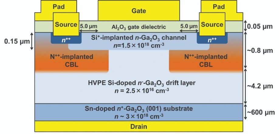
Figure 4. The vertical D-mode Ga2O3 MOSFET pioneered by NICT.
Our D-mode MOSFET has a GaN current-aperture vertical electron transistor (CAVET) structure (the cross-section is shown in Figure 4). We make this by taking an n+-Ga2O3 (001) bulk substrate, loading it in a halide vapor phase epitaxy (HVPE) reactor, and adding a drift layer with a silicon doping concentration of 2.5×1016 cm-3. Devices are then formed using three ion-implantation processes. This creates a p-Ga2O3 current-blocking layer, followed by an n-Ga2O3 channel, and n+-Ga2O3 ohmic contacts. Secondary-ion mass spectrometry measurements on this structure reveal the depth profiles for the silicon and nitrogen atoms, and validate the fabrication process (see Figure 5).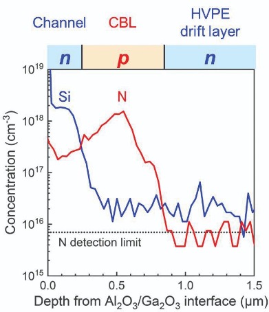
Figure 5. Depth profiles of implanted silicon and nitrogen atom concentrations in the overlapping region of the gate metal and the current-blocking layer of a vertical Ga2O3 MOSFET structure measured by secondary-ion mass spectrometry (SIMS). These data were obtained from a completed device. The depth profiles of both silicon and nitrogen atoms were just as designed.
Plotting DC current-voltage output characteristics and transfer characteristics of our MOSFET reveals its decent device characteristics (see Figure 6). These transistors have a maximum drain current density of 0.42 kA cm-2, a specific on-resistance of 31.5 mΩ·cm2, and a high drain-current on/off ratio – it is over eight orders of magnitude. The off-state breakdown voltage in these MOSFETs is limited to less than 30 V, due to a large electric field in the Al2O3 gate dielectric. However, this can be increased by improving the material quality of the gate dielectric and optimising doping.While there is still much room left to improve the performance of our vertical MOSFETs, they are a breakthrough. The real value of this accomplishment lies in the use of multiple n- and p-type ion implantations to fabricate these vertical transistors, mirroring the process for making silicon and SiC devices. In other words, we have established a baseline process for future mass production of Ga2O3 power devices, and this greatly enhances the commercial prospects of this class of device.
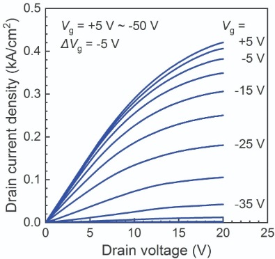
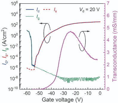
Figure 6. (a) DC output characteristics and (b) transfer characteristics of vertical Ga2O3 MOSFET.
What next?Thanks to the high thermal stability of nitrogen in Ga2O3, there are unique opportunities for designing and engineering a variety of high-voltage Ga2O3 devices. It is worth noting that the p-type behaviour of nitrogen-doped Ga2O3 has also been observed for MBE-grown materials, in which nitrogen atoms are incorporated during epitaxial growth. However, many of the material properties of nitrogen-doped Ga2O3 are still unknown. It is also unclear how nitrogen atoms are incorporated in Ga2O3 lattice sites. Frankly, it is counter-intuitive to imagine that a nitrogen atom would displace and replace an oxygen atom in the Ga2O3 lattice, as an oxygen ion is very electronegative and its 2p orbitals are very stable. However, this picture is necessary to explain the activation of nitrogen atoms as acceptors.
Our work is helping Ga2O3 to rapidly emerge as the next major wide-bandgap semiconductor. In just the last few years, Ga2O3 transistors have taken enormous strides, such as the demonstration of kilovolt breakdown, normally-off operation, and the capability to form vertical devices. These breakthroughs are helping to position Ga2O3 as a strong contender for future technologies.
What’s needed now is to transfer the Ga2O3
transistors and diodes from the lab to the fab, so that commercial devices can start serving in practical applications. With the full support of the research community, which is establishing a more complete understanding of the materials and devices, this is a goal that can be reached by efforts directed at developing and building up the technologies. This will take time, but the payback will more than justify all the effort.
Masataka Higashiwaki and Man Hoi Wong thank Dr. Ken Goto, Prof. Hisashi Murakami, and Prof. Yoshinao Kumagai of Tokyo University of Agriculture and Technology for their collaborative contributions to HVPE growth in this work. This work was partially supported by Council for Science, Technology and Innovation (CSTI), Cross-ministerial Strategic Innovation Promotion Program (SIP), “Next-generation power electronics” (funding agency: New Energy and Industrial Technology Development Organization).
Further reading
M. Higashiwaki and G. H. Jessen. Appl. Phys. Lett. 112 060401 (2018)
A. Kuramata et al. Jpn. J. Appl. Phys. 55 1202A2 (2016)
M. Higashiwaki et al. Appl. Phys. Lett. 100 013504 (2012)
K. Sasaki et al. Appl. Phys. Express 6 086502 (2013)
M. H. Wong et al. Appl. Phys. Lett. 113 102103 (2018)
M. H. Wong et al. IEEE Electron Device Lett. 40 431 (2019)













.jpeg)


